PTFA240451E
Thermally-Enhanced High Power RF LDMOS FET
45 W, 2420 – 2480 MHz
Description
The PTFA240451E is a thermally-enhanced, 45-watt, internallymatched GOLDMOS® FET intended for CDMA2000 and WiMAX
applications from 2420 to 2480 MHz. Thermally-enhanced packaging
provides the coolest operation available. Full gold metallization
ensures excellent device lifetime and reliability.
Features
• Thermally-enhanced, lead-free and
RoHS-compliant packaging
Three-Carrier CDMA2000 Performance
VDD = 28 V, IDQ = 450 mA, ƒ = 2450 MHz
Efficiency
ACP Up
ACP Low
ALT Up
Drain Efficiency (%)
40
35
-38
-42
-46
30
-50
25
-54
20
-58
15
-62
Efficiency
10
-66
5
-70
0
-74
30
32
34
36
38
40
Adj. Ch. Power Ratio (dBc)
45
PTFA240451E
Package H-30265-2
42
Output Power, Avg. (dBm)
•
Broadband internal matching
•
Typical two-carrier CDMA performance at 2450
MHz, 28 V
- Average output power = 10 W
- Linear Gain = 14 dB
- Efficiency = 27%
- Adjacent channel power = –45 dBc
•
Typical CW performance, 2450 MHz, 28 V
- Output power at P–1dB = 50 W
- Efficiency = 54%
•
Integrated ESD protection: Human Body Model,
Class 2 (minimum)
•
Excellent thermal stability, low HCI drift
•
Capable of handling 10:1 VSWR @ 28 V,
45 W (CW) output power
RF Characteristics
3-Carrier CDMA2000 Measurements (not subject to production test—verified by design/characterization in Infineon test fixture)
VDD = 28 V, IDQ = 450 mA, POUT = 14 W average, ƒ = 2450 MHz, channel bandwidth = 3.75 MHz; ACPR measured in 30 kHz
bandwidth at ƒC ± 2.135 MHz offset
Characteristic
Symbol
Min
Typ
Max
Unit
Gain
Gps
—
14
—
dB
Drain Efficiency
ηD
—
31
—
%
ACPR
—
–45
—
dBc
Adjacent Channel Power Ratio
All published data at TCASE = 25°C unless otherwise indicated
*See Infineon distributor for future availability.
ESD: Electrostatic discharge sensitive device—observe handling precautions!
Data Sheet
1 of 10
Rev. 04, 2008-03-04
�PTFA240451E
RF Characteristics (cont.)
Two-tone Measurements (tested in Infineon test fixture)
VDD = 28 V, IDQ = 450 mA, POUT = 45 W PEP, ƒ = 2480 MHz, tone spacing = 1 MHz
Characteristic
Symbol
Min
Typ
Max
Unit
Gain
Gps
13.5
14
—
dB
Drain Efficiency
ηD
39
40
—
%
Intermodulation Distortion
IMD
—
–30
–28
dBc
DC Characteristics
Characteristic
Conditions
Symbol
Min
Typ
Max
Unit
Drain-Source Breakdown Voltage
VGS = 0 V, IDS = 10 mA
V(BR)DSS
65
—
—
V
Drain Leakage Current
VDS = 28 V, V GS = 0 V
IDSS
—
—
1.0
µA
VDS = 63 V, V GS = 0 V
IDSS
—
—
10.0
µA
RDS(on)
—
0.17
—
Ω
On-State Resistance
VGS = 10 V, V DS = 0.1 V
Operating Gate Voltage
VDS = 28 V, IDQ = 450 mA
VGS
2.0
2.5
3.0
V
Gate Leakage Current
VGS = 10 V, V DS = 0 V
IGSS
—
—
1.0
µA
Maximum Ratings
Parameter
Symbol
Value
Unit
Drain-Source Voltage
VDSS
65
V
Gate-Source Voltage
VGS
–0.5 to +12
V
Junction Temperature
TJ
200
°C
Total Device Dissipation
PD
196
W
1.12
W/°C
Above 25°C derate by
Storage Temperature Range
TSTG
–40 to +150
°C
Thermal Resistance (TCASE = 70°C, 45 W CW)
RθJC
0.89
°C/W
Ordering Information
Type and Version
Package Outline
Package Description
Marking
PTFA240451E
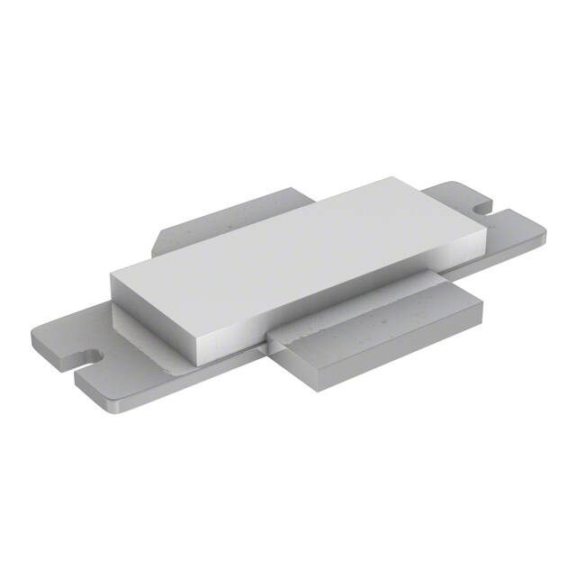
H-30265-2
Thermally-enhanced slotted flange, single-ended
PTFA240451E
Data Sheet
V1
2 of 10
Rev. 04, 2008-03-04
�PTFA240451E
Typical Performance (data taken in a production test fixture)
Typical POUT, Gain & Efficiency (at P-1dB)
vs. Frequency
Intermodulation Distortion vs. Output Power
(as measured in a broadband circuit)
VDD = 28 V, IDQ = 450 mA, ƒ1 = 2449 MHz, ƒ 2 = 2450 MHz
-20
57
16
Efficiency
-30
5th Order
Gain (dB)
IMD (dBc)
-40
-50
-60
7th Order
Gain
13
-80
32
34
36
38
40
42
53
14
-70
30
55
15
3rd Order
12
2420
44
51
Output Power
2430
2440
2450
2460
2470
49
2480
Efficiency (%), Output Power (W)
VDD = 28 V, IDQ = 450 mA
Frequency (MHz)
Output Power, Avg. (dBm)
IM3 vs. Output Power for Selected Biases
2-Tone Broadband Performance
VDD = 28 V, ƒ 1 = 2449 MHz, ƒ 2 = 2450 MHz
VDD = 28 V, IDQ = 450 mA, POUT Avg. = 43.52 dBm
-20
50
-5
337 m A
-40
-50
562 m A
450 m A
-60
-70
30
32
34
36
38
40
42
-10
30
-15
20
-20
Gain
10
-25
Return Loss
0
2400
44
Output Power, Avg. (dBm )
Data Sheet
40
Return Loss (dB)
IMD (dBc)
-30
Gain (dB), Efficiency (%)
Efficiency
2420
2440
2460
2480
-30
2500
Frequency (MHz)
3 of 10
Rev. 04, 2008-03-04
�PTFA240451E
Typical Performance (cont.)
Power Sweep
Gain & Efficiency vs. Output Power
VDD = 28 V, ƒ = 2450 MHz
VDD = 28 V, IDQ = 450 mA, ƒ = 2450 MHz
IDQ = 675 mA
50
15
15.0
Gain
14.5
IDQ = 450 mA
13.5
14
40
13
30
12
12.5
20
Efficiency
13.0
10
11
IDQ = 225 mA
12.0
0
10
30
32
34
36
38
40
42
44
46
48
30
34
Output Power (dBm)
38
46
50
Output Power (dBm)
IS-95 CDMA Performance
Output Power (at 1 dB Compression)
vs. Supply Voltage
VDD = 28 V, IDQ = 450 mA, ƒ = 2450 MHz
IDQ = 450 mA, ƒ = 2450 MHz
TCASE = 25°C
TCASE = 90°C
35
49
Drain Efficiency (%)
48
47
46
-35
ACP ƒ C–0.75 MHz
30
Output Power (dBm)
42
-40
-45
25
Efficiency
-50
20
-55
15
-60
10
-65
5
-70
ACPR ƒ C+1.98 MHz
0
45
24
26
28
30
Supply Voltage (V)
Data Sheet
-75
30
32
32
34
36
38
40
Adj. Channel Power Ratio (dBc)
14.0
Gain (dB)
Power Gain (dB)
60
16
15.5
Drain Efficiency (%)
16.0
42
Output Power, Avg. (dBm)
4 of 10
Rev. 04, 2008-03-04
�PTFA240451E
Typical Performance (cont.)
WiMAX Performance
VDD = 28 V, IDQ = 0.45 A,
(modulation = 64 QAM2/3, channel bandwidth = 3.5 MHz,
sample rate = 4 MHz)
36
-15
Efficiency
30
-20
ƒ = 2.62 GHz
ƒ = 2.68 GHz
24
-25
ƒ = 2.65 GHz
0.09 A
0.28 A
1.02
0.46 A
1.01
0.70 A
1.00
1.39 A
0.99
2.09 A
Efficiency (%)
Normalized Bias Voltage (V)
1.03
2.78 A
0.98
3.48 A
0.97
18
-30
12
-35
6
-40
EVM (dBc)
Bias Voltage vs. Temperature
Voltage normalized to typical gate voltage,
series show current
4.17 A
0.96
0.95
-20
0
0
20
40
60
80
100
-45
15
Case Temperature (°C)
20
25
30
35
40
45
Output Power (dBm)
WiMAX Performance
VDD = 28 V, ƒ = 2450 MHz
(modulation = 64 QAM2/3, channel bandwidth = 3.5 MHz,
sample rate = 4 MHz)
-15
EVM (dB)
-20
IDQ = 0.28 A
-25
IDQ = 0.67 A
-30
-35
IDQ = 0.45 A
-40
-45
15
20
25
30
35
40
45
Output Power (dBm)
Data Sheet
5 of 10
Rev. 04, 2008-03-04
�PTFA240451E
Broadband Circuit Impedance
Z Source Ω
Frequency
jX
2400
22.12
–18.74
6.98
–2.35
2420
20.27
–18.71
6.73
–2.14
2450
18.30
–19.18
6.61
–2.17
2480
15.24
–19.95
6.17
–2.32
2500
13.45
–20.19
5.92
–2.41
Z Load
2500 MHz
0.5
R
0.1
0 .0
DT OW ARD L OA
GTHS
E LEN
jX
2400 MHz
0.1
Z Source
WAV


 工商网监
湘ICP备2023018690号
工商网监
湘ICP备2023018690号
